65V, 6A high-power density buck module with mitigated interference and noise technology
Texas Instruments
 RSS
Sample
RSS
Sample
- Darmowa próbka
- MPN:
- TPSM65660
- Producent:
- TEXAS INSTRUMENTS
- Dodany do bazy:
- Ostatnio widziany:
Sugerowane produkty dla cyclebycycle
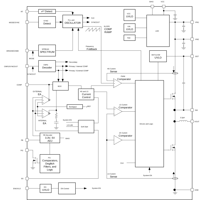
The TPSM656x0 is a
synchronous, buck DC/DC power module offered from a family of modules with mitigated
interference and noise technology using architecture 2 features (MINT 2) that
combines a controller, power MOSFETs, and a power inductor in a 31-pin enhanced
HotRod QFN package for easy implementation of high-efficiency, high power density,
low electromagnetic interference (EMI) designs. The modules operate over a wide
input voltage range of 3.5V to 65V simplifying input surge protection design.
Phase stackable with synchronized
interleaving, the peak current-mode control architecture of the TPSM656x0 supports accurate current sharing with
paralleled phases for higher output currents. Auto mode enables frequency foldback
during light-load operation, giving high light-load efficiency, which extends
run-time in battery-powered systems.
A high-side switch minimum on-time of
36ns facilitates large step-down ratios, enabling the direct conversion from 24V or
48V inputs to low-voltage rails for reduced system cost and complexity. The package
has several NC pins between critical power pins, improving the Failure Modes and
Effects Analysis (FMEA) results.
The TPSM656x0 includes several features to simplify
compliance with CISPR 11 and CISPR 32 emissions requirements. First, a symmetrical
pinout provides excellent input capacitor placement and, together with integrated
high-frequency input capacitors, enables an ultra-low effective value for the
power-loop parasitic inductance, which reduces switching losses and improves EMI
performance at high input voltage and high switching frequency. A pin-selectable
switch-node slew-rate control feature further reduces emissions at high frequencies.
To lower input capacitor ripple current and EMI filter size, interleaved operation
using a SYNCOUT signal with 180° phase shift works well for cascaded, multichannel
or multiphase designs. Resistor-adjustable switching frequency as high as 2.2MHz can
be synchronized to an external clock source to eliminate beat frequencies in
noise-sensitive applications. Finally, the TPSM656x0 has
dual-random spread spectrum (DRSS), which is a unique EMI-reduction feature that
combines low-frequency triangular and high-frequency random modulations to mitigate
disturbances across lower and higher frequency bands, respectively.
Additional
features of the TPSM656x0 include 150°C maximum junction
temperature operation, open-drain power-good (PG) indicator for fault reporting and
output voltage monitoring, precision enable input for input UVLO protection,
monotonic start-up into prebiased loads, dual-input VCC bias subregulator powered
from VIN or BIAS, hiccup-mode overload protection, and thermal shutdown protection
with automatic recovery.
The TPSM656x0 comes in a 4.2mm × 7.7mm, thermally enhanced,
31-pin eQFN package with additional pin clearance for increased reliability.
Leveraging a flip-chip routable leadframe (FCRLF) packaging technique, the TPSM656x0 with useable current, lifetime reliability, and
cost advantages targets applications requiring high power density. The wide input
voltage range, low quiescent current consumption, high-temperature operation,
cycle-by-cycle current limit, low EMI signature, and small design size provide an
excellent point-of-load regulator design for applications requiring enhanced
robustness and durability.
Elecena nie prowadzi sprzedaży elementów elektronicznych, ani w niej nie pośredniczy.
Produkt pochodzi z oferty sklepu Texas Instruments