1.8 V, 6 LVDS/12 CMOS Outputs Low Power Clock Fanout Buffer
Analog Devices
 RSS
Sample
RSS
Sample
- Darmowa próbka
- MPN:
- ADCLK846
- Producent:
- ANALOG DEVICES
- Dodany do bazy:
- Ostatnio widziany:
- Zmiana ceny:
- -100% (18.01.2025)
- Poprzednia cena:
- 5.14
Sugerowane produkty dla adclk846
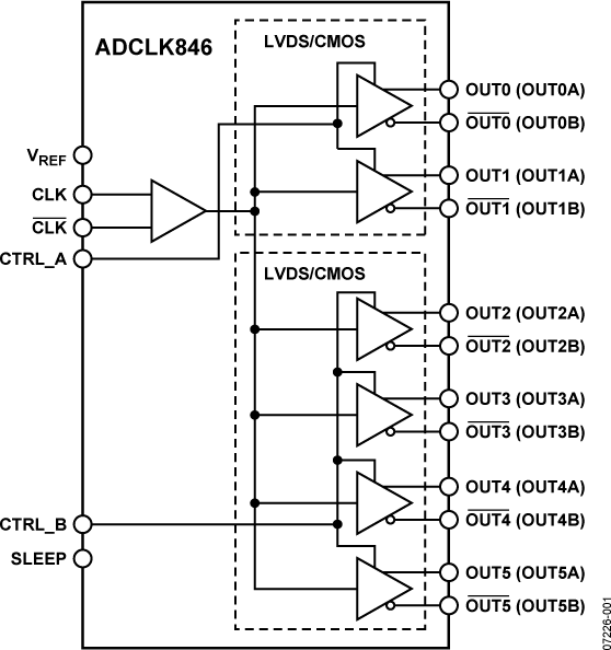
The ADCLK846 is a 1.2 GHz/250 MHz, LVDS/CMOS, fanout buffer optimized for low jitter and low power operation. Possible configurations range from 6 LVDS to 12 CMOS outputs, including combinations of LVDS and CMOS outputs. Two control lines are used to determine whether fixed blocks of outputs are LVDS or CMOS outputs.
The clock input accepts various types of single-ended and differential logic levels including LVPECL, LVDS, HSTL, CML, and CMOS.
Table 8 provides interface options for each type of connection. The SLEEP pin enables a sleep mode to power down the device.
This device is available in a 24-pin LFCSP package. It is specified for operation over the standard industrial temperature range of −40°C to +85°C.
APPLICATIONS
* Low jitter clock distribution
* Clock and data signal restoration
* Level translation
* Wireless communications
* Wired communications
* Medical and industrial imaging
* ATE and high performance instrumentation
* Selectable LVDS/CMOS outputs
* Up to 6 LVDS (1.2 GHz) or 12 CMOS (250 MHz) outputs
* <16 mW per channel (100 MHz operation)
* 54 fs integrated jitter (12 kHz to 20 MHz)
* 100 fs additive broadband jitter
Elecena nie prowadzi sprzedaży elementów elektronicznych, ani w niej nie pośredniczy.
Produkt pochodzi z oferty sklepu Analog Devices