Low Frequency to 3 GHz, Dual VGA with Output Common-Mode and DC Offset Control
Analog Devices
 RSS
Sample
RSS
Sample
- Darmowa próbka
- MPN:
- ADRF6521
- Producent:
- ANALOG DEVICES
- Dodany do bazy:
- Ostatnio widziany:
- Zmiana ceny:
- -100% (17.01.2025)
- Poprzednia cena:
- 18.35
Sugerowane produkty dla is100
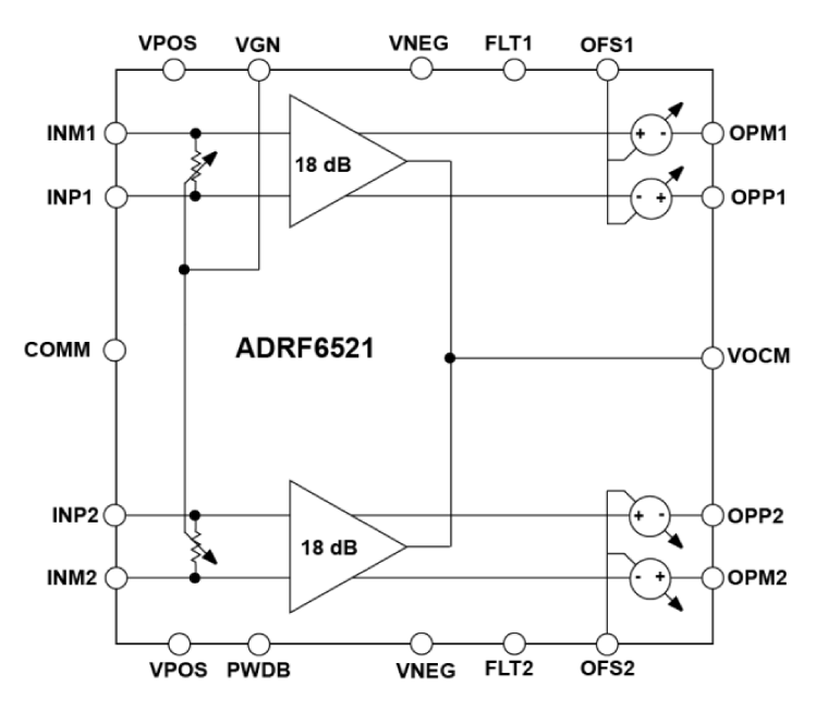
The ADRF6521 is a dual, fully differential, low noise and low distortion variable gain amplifier (VGA). The high spurious-free dynamic range over the gain range makes the ADRF6521 ideal for communication systems with dense constellations, multiple carriers, and nearby interferers.
The VGA has a 21 dB attenuation range with a typical voltage gain of 18 dB. The differential input impedance is 100 Ω, while the differential output impedance is 16 Ω. The ±1 dB gain flatness bandwidth is 2.5 GHz. The output buffers are capable of swinging 1.5 V p-p into 100 Ω loads at >55 dBc for second-order and third-order intermodulation distortion (IMD2 and IMD3), and for second and third harmonic distortion (HD2 and HD3) from low frequency to 1 GHz. Variable output dc offset control is accomplished with the OFS1 and OFS2 pins, and the output common-mode can be controlled with the VOCM pin.
The ADRF6521 flexibly operates from a single +5 V supply or from a range of dual supplies and consumes a total supply current of 200 mA. When fully disabled, it consumes 25 mA typical. The ADRF6521 is fabricated in an advanced silicon-germanium BiCMOS process and is available in a 20-lead, exposed pad, 3 mm × 3 mm LFCSP. Performance is specified over the −40°C to +85°C temperature range.
Applications
* Point-to-point and point-to-multipoint radios
* Baseband IQ receivers
* Diversity receivers
* ADC drivers
* Instrumentation
* Medical
* Dual, matched VGAs
* Maximum voltage gain: 18 dB
* Gain control attenuation range: 21 dB typical for TA = 25°C
* ±1 dB gain flatness bandwidth: 2.5 GHz typical
* IMD2 and IMD3 (1.5 V p-p output level)
* −56.8 dBc typical and −75 dBc typical, respectively, at VGN = 1.5 V, 980 MHz and 1000 MHz tones
* HD2 and HD3 (1.5 V p-p output level)
* −75 dBc typical and −73.7 dBc typical, respectively, at VGN = 1.5 V, fundamental at 500 MHz
* −55.9 dBc typical and −57.5 dBc typical, respectively, at VGN = 1.5 V, fundamental at 1 GHz
* Noise figure:
* 10.5 dB typical at maximum gain and at 500 MHz
* 14.8 dB at maximum gain and at 2 GHz
* Noise figure decreases dB for dB with gain backoff
Elecena nie prowadzi sprzedaży elementów elektronicznych, ani w niej nie pośredniczy.
Produkt pochodzi z oferty sklepu Analog Devices