Precision Analog Microcontroller, 12-Bit Analog Input/Output, ARM7TDMI MCU
Analog Devices
 RSS
Sample
RSS
Sample
- Darmowa próbka
- MPN:
- ADUC7120
- Producent:
- ANALOG DEVICES
- Dodany do bazy:
- Ostatnio widziany:
- Zmiana ceny:
- -100% (20.01.2025)
- Poprzednia cena:
- 19.42
Sugerowane produkty dla aduc7120
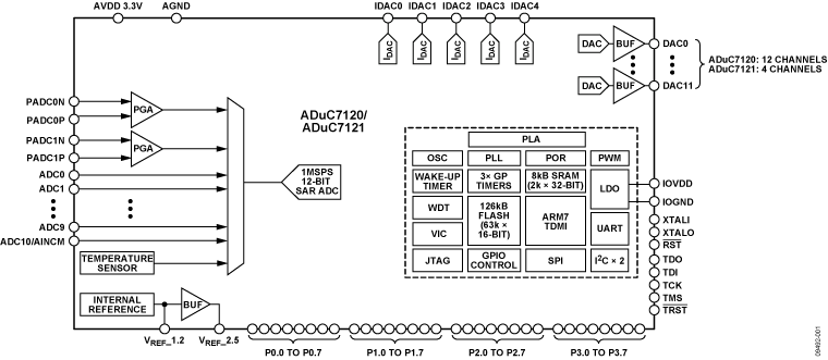
The ADuC7120/ADuC7121 are fully integrated, 12-bit, 1 MSPS, data acquisition systems incorporating a high performance multichannel ADC, 16-bit/32-bit microcontroller unit (MCU), and Flash®/EE memory on a single chip.
The analog-to-digital converter (ADC) consists of eleven single-ended inputs for the ADuC7120 (seven single-ended inputs for the ADuC7121) and two extra differential input pairs. The two differential input pairs can be routed through a programmable gain amplifier (PGA). The ADC can operate in single-ended or differential input mode. The ADC input voltage is 0 V to VREF. A low drift band gap reference, temperature sensor, and voltage comparator complete the ADC peripheral set.
The ADuC7120/ADuC7121 provide five current output digital-to-analog converters (DACs). The current sources (five current DACs) feature low noise and low drift, high-side current output at an 11-bit resolution. The five current digital-to-analog converters (IDACs) are as follows: IDAC0 with 250 mA full-scale (FS) output, IDAC1 with 200 mA FS output, IDAC2 with 45 mA FS output, IDAC3 with 80 mA FS output, and IDAC4 with 20 mA FS output.
The ADuC7120/ADuC7121 also contain up to 12 voltage output DACs. The DAC output range is programmable to one of three voltage ranges.
The devices operate from an on-chip oscillator and a phase-locked loop (PLL) generating an internal high frequency clock of 41.78 MHz (UCLK). This clock is routed through a programmable clock divider from which the MCU core clock operating frequency is generated. The microcontroller core is an ARM7TDMI®, 16-bit/32-bit reduced instruction set computer (RISC) machine, which offers up to 41 MIPS peak performance. 8 kB of SRAM and 126 kB of nonvolatile Flash/EE memory are provided on chip. The ARM7TDMI core views all memory and registers as a single linear array.
On-chip factory firmware supports in circuit serial download via the I2C serial interface port; nonintrusive emulation is also supported via the JTAG interface. These features are incorporated into a low cost QuickStart development system supporting this MicroConverter® family.
The devices operate from 3.0 V to 3.6 V, and they are specified over the −40°C to +105°C industrial temperature range. The IDACs are powered from a separate input power supply, PVDD. When operating at 41.78 MHz, the power dissipation is typically 120 mW. The ADuC7120/ADuC7121 are available in a 108-ball chip-scale package ball grid array [CSPBGA].
Applications
* Optical modules—tunable laser
* Analog input/output
* Multiple channel, 12-bit, 1 MSPS ADC
* 2 differential pairs with input PGA
* General-purpose inputs (differential or single-ended)
* ADuC7120: 11 channels
* Fully differential and single-ended modes
* 0 V to VREF analog input voltage range (single-ended mode)
* 5 low noise IDACs
* 250 mA, 200 mA, 45 mA, 80 mA, 20 mA
* 12-bit voltage output DACs
* ADuC7120: 12 channels
* 4× 12-bit voltage output DACs
* On-chip voltage reference
* On-chip temperature sensor
* Microcontroller
* ARM7TDMI core, 16-bit/32-bit RISC architecture
* JTAG port supports code download and debug
* Clocking options
* Trimmed on-chip oscillator (±3%)
* External watch crystal
* External clock source up to 41.78 MHz
* 41.78 MHz PLL with programmable divider
* Memory
* 126 kB Flash/EE memory, 8 kB SRAM
* In-circuit download, JTAG-based debug
* Software triggered in-circuit reprogrammability
* On-chip peripherals
* UART, 2 × I2C and SPI serial I/O
* 32-pin GPIO port
* 4× general-purpose timers
* Wake-up timers and WDT
* Power supply monitor
* IDAC monitor
* Temperature monitor
* Vectored interrupt controller for FIQ and IRQ
* 8 priority levels for each interrupt type
* Interrupt on edge or level external pin inputs
* Power
* Specified for 3 V operation
* Normal mode: 11 mA at 5.22 MHz, 30 mA at 41.78 MHz
* Packages and temperature range
* 7 mm × 7 mm 108-ball CSPBGA
* Fully specified for –40°C to +105°C operation
* Tools
* Low cost QuickStart development system
* Full third party support
Elecena nie prowadzi sprzedaży elementów elektronicznych, ani w niej nie pośredniczy.
Produkt pochodzi z oferty sklepu Analog Devices