3 V/5 V Low Power, Synchronous Voltage-to-Frequency Converter
Analog Devices
 RSS
Sample
RSS
Sample
- Darmowa próbka
- MPN:
- AD7740
- Producent:
- ANALOG DEVICES
- Dodany do bazy:
- Ostatnio widziany:
- Zmiana ceny:
- -100% (20.01.2025)
- Poprzednia cena:
- 1.16
Sugerowane produkty dla ad7740
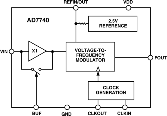
The AD7740 is a low-cost, ultrasmall synchronous Voltage-to-Frequency Converter (VFC). It works from a single 3.0 V to 3.6 V or 4.75 V to 5.25 V supply consuming 0.9 mA. The AD7740 is available in an 8-lead SOT-23 and also in an 8-lead MSOP package. Small package, low cost and ease of use were major design goals for this product. The part contains an on-chip 2.5 V bandgap reference but the user may overdrive this using an external reference. This external reference range includes VDD.
The full-scale output frequency is synchronous with the clock signal on the CLKIN pin. This clock can be generated with the addition of an external crystal (or resonator) or supplied from a CMOS-compatible clock source. The part has a maximum input frequency of 1 MHz.
For an analog input signal that goes from 0 V to VREF, the output frequency goes from 10% to 90% of fCLKIN. In buffered mode, the part provides a very high input impedance and accepts a range of 0.1 V to VDD – 0.2 V on the VIN pin. There is also an unbuffered mode of operation that allows VIN to go from –0.15 V to VDD + 0.15 V. The modes are interchangeable using the BUF pin.
The AD7740 (Y Grade) is guaranteed over the automotive temperature range of –40°C to +105°C. The AD7740 (K Grade) is guaranteed from 0°C to 85°C.
Product Highlights
* The AD7740 is a single channel, single-ended VFC. It is
available in 8-lead SOT-23 and 8-lead MSOP packages, and is
intended for low-cost applications. The AD7740 offers
considerable space saving over alternative solutions.
* The AD7740 operates from a single 3.0 V to 3.6 V or 4.75 V
to 5.25 V supply and consumes typically 0.9 mA when the
input is unbuffered. It also contains an automatic power-down
function.
* The AD7740 does not require external resistors and capacitors
to set the output frequency. The maximum output
frequency is set by a crystal or a clock. No trimming or calibration
is required.
* The analog input can be taken to 150 mV below GND for
true bipolar operation.
* The specified voltage reference range on REFIN is from
2.5 V to the supply voltage, VDD.
Applications
* Isolation of high common-mode voltages
* Low-cost analog-to-digital conversion
* Battery monitoring
* Automotive sensing
* Synchronous operation
* Full-scale frequency set by external system clock
* 8-lead SOT-23 and 8-lead MSOP packages
* 3 V or 5 V operation
* Low power: 3 mW (Typ)
* Nominal input range: 0 to VREF
* True –150 mV capability without charge pump
* VREF range: 2.5 V to VDD
* Internal 2.5 V reference
* 1 MHz max input frequency
* Selectable high impedance buffered input
* Minimal external components required
Elecena nie prowadzi sprzedaży elementów elektronicznych, ani w niej nie pośredniczy.
Produkt pochodzi z oferty sklepu Analog Devices