12-Bit, 4GSPS, JESD204B/C, Quad Analog-to-Digital Converter
Analog Devices
 RSS
Sample
- Darmowa próbka
- MPN:
- AD9209
- Producent:
- ANALOG DEVICES
- Dodany do bazy:
- Ostatnio widziany:
- Zmiana ceny:
- -100% (20.01.2025)
- Poprzednia cena:
- 1115.51
Sugerowane produkty dla ad9209
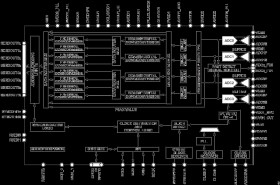
The AD9209 is a quad, 12-bit, 4 GSPS analog-to-digital converter (ADC). The ADC input features an on-chip wideband buffer with overload protection. This device is designed to support applications capable of direct sampling wideband signals up to 8 GHz. An on-chip, low phase noise, phase-locked loop (PLL) clock synthesizer is available to generate the ADC sampling clock, simplifying the printed circuit board (PCB) distribution of a high frequency clock signal. A clock output buffer is available to transmit the ADC sampling clock to other devices.
The quad ADC cores have code error rates (CER) better than 1 × 10⁻²⁰. Low latency fast detection and signal monitoring are available for automatic gain control (AGC) purposes. A flexible 192-tap programmable finite impulse response filter (PFIR) is avail-able for digital filtering and/or equalization. Programmable integer and fractional delay blocks support compensation for analog delay mismatches.
The digital signal processing (DSP) block consisting of two coarse digital down converters (DDCs) and four fine DDCs per pair of ADCs. Each ADC can operate with one or two main DDC stages in support of multiband applications. The four additional fine DDC stages are available to support up to four bands per ADC The 48-bit numerically controlled oscillators (NCOs) associated with each DDC support fast frequency hopping (FFH) while maintaining synchronization with up to 16 unique frequency assignments selected via the general-purpose input and output (GPIOx) pins or the serial port interface (SPI).
The AD9209 supports one or two JTx links that can be configured for either JESD204B or JESD204C subclass operation, thus allowing for different datapath configurations for each ADC. Multidevice synchronization is supported through the SYSREF± input pins.
APPLICATIONS
* Wireless communications infrastructure
* Microwave point-to-point, E-band, and 5G mm wave
* Broadband communications systems
* DOCSIS 3.1 and 4.0 CMTS
* Phased array radar and electronic warfare
* Electronic test and measurement systems
* Flexible reconfigurable common platform design
* Supports single-, dua-l, and quad-band
* Datapaths and DSP blocks are fully bypassable
* On-chip PLL with multichip synchronization
* External RF clock input option for off-chip PLL
* Supports clock input frequencies up to 12 GHz
* Maximum ADC sample rate up to 4 GSPS
* Maximum data rate up to 4 GSPS using JESD204C
* 8 GHz analog input bandwidth (−3 dB)
* ADC ac performance at 4 GSPS
* Differential input voltage: 1.4 V p-p
* Noise density: −151.5 dBFS/Hz
* HD2: −69 dBFS at 2.7 GHz (AIN at −1 dBFS)
* HD3: −76 dBFS at 2.7 GHz (AIN at −1 dBFS)
* Worst other (excluding HD2 and HD3): −79 dBFS at 2.7 GHz
* Auxiliary features
* Phase coherent fast frequency hopping
* ADC clock driver with selectable divide ratios
* On-chip temperature monitoring unit
* Flexible GPIOx pins
Elecena nie prowadzi sprzedaży elementów elektronicznych, ani w niej nie pośredniczy.
Produkt pochodzi z oferty sklepu Analog Devices