16-Bit, ±1 LSB Accuracy Voltage Output DAC with SPI Interface
Analog Devices
 RSS
Sample
RSS
Sample
- Darmowa próbka
- MPN:
- MAX5316
- Producent:
- ANALOG DEVICES
- Dodany do bazy:
- Ostatnio widziany:
- Zmiana ceny:
- -100% (19.01.2025)
- Poprzednia cena:
- 12.49
Sugerowane produkty dla max5317
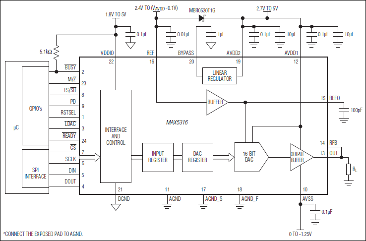
The MAX5316 is a high-accuracy, 16-bit, serial SPI input, buffered voltage output digital-to-analog converter (DAC) in a 4mm x 5mm, 24-lead TQFN package. The device features ±1 LSB INL (max) accuracy and a ±0.25 LSB DNL (typ) accuracy over the temperature range of -40°C to +105°C.
The DAC voltage output is buffered with a fast settling time of 3µs and a low offset and gain drift of ±0.6ppm/°C of FSR (typ). The force-sense output (OUT) maintains accuracy while driving loads with long lead lengths. A separate AVSS supply is provided to permit the output amplifier to go to 0V (GND) to maintain full linearity performance near ground.
At power-up, the device resets its outputs to zero or midscale.
The wide 2.7V to 5.5V supply voltage range and integrated low-drift, low-noise reference buffer make for ease of use. The MAX5316 features a 50MHz 3-wire SPI interface. For an I²C interface, use the MAX5317.
The MAX5316 is available in a 24-lead TQFN-EP package and operates over the -40°C to +105°C temperature range.
Applications
* Automatic Calibration * Automatic Test Equipment * Communication Systems * Data-Acquisition Systems * Gain and Offset Adjustment * Medical Equipment * Process Control and Servo Loops * Programmable Voltage and Current Sources * Test and Measurement
* Ideal for ATE and High-Precision Instruments
* INL Accuracy Guaranteed with ±1 LSB (Max) Over Temperature
* Fast Settling Time (3µs) with 10kΩ || 100pF Load
* Safe Power-Up-Reset to Zero or Midscale DAC Output (Pin-Selectable)
* Predetermined Output Device State in Power-Up and Reset in System Design
* Negative Supply (AVSS) Option Allows Full INL/DNL Performance to 0V
* SPI Interface Compatible with 1.7V to 5.5V Logic
* High Integration Reduces Development Time and PCB Area
* Buffered Voltage Output Directly Drives 2kΩ Load Rail-to-Rail
* Integrated Reference Buffer
* No External Amplifiers Required
* Small 4mm × 5mm, 24-Pin TQFN Package
Elecena nie prowadzi sprzedaży elementów elektronicznych, ani w niej nie pośredniczy.
Produkt pochodzi z oferty sklepu Analog Devices